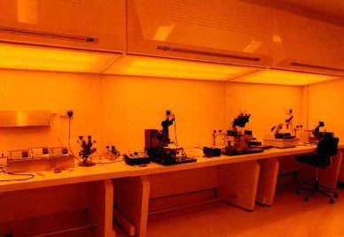
University of Essex Nanofab
These pages provide an overview of the semiconductor device research and teaching nanofabrication facilities
References & Acknowledgements
Dr Geoff Hill
Device Fabrication EPSRC III-V Semiconductor Central Facility
Addison Wesley 1990 John Wiley 1983 Cahners Publishing PennWell Publishing PennWell Publishing http://cr.pennnet.com/home/home.cfm PennWell Publishing Adam Hilger 1990 These pages are written & maintained by Adrian Boland-Thoms
Guide to Etching
Techniques
Modern Gallium Arsenide Processing Techniques 2nd ed (Artech House
1990)
R.E.Williams
Semiconductors & Electronic Devices (Prentice Hall
1987)
Adir Bar-Lev
Introduction to Semiconductors
Bart J. Van Zeghbroeck, 1996, 1997
Semiconductor
Integrated Circuit Processing Technology
W.R.Runyan, K.E.Bean (Texas
Instruments)
VLSI
Fabrication Principles: Silicon & Gallium Arsenide
Sorab K. Gandhi
Semiconductor
International http://209.67.253.149/
The Industry's
Source Book for Processing, Assembly & Testing
Solid State
Technology
Worldwide
Semiconductor Production
EuroPhotonics
http://www.europhotonics.com/
Laurin Publishing
European coverage
of product developments in optics, imaging, fibre optics, electro-optics and
optoelectronics
Laser Focus
World http://lfw.pennwellnet.com/home/home.cfm
Advances in
Optics, Electro-optics, and Optoelctronics
Cleanrooms
International
The international
magazine of contamination control technology
Growth and
Characterisation of Semiconductors
ed.R.,A.Stradling
& P.C.Klipstein
