University of Essex Nanofab

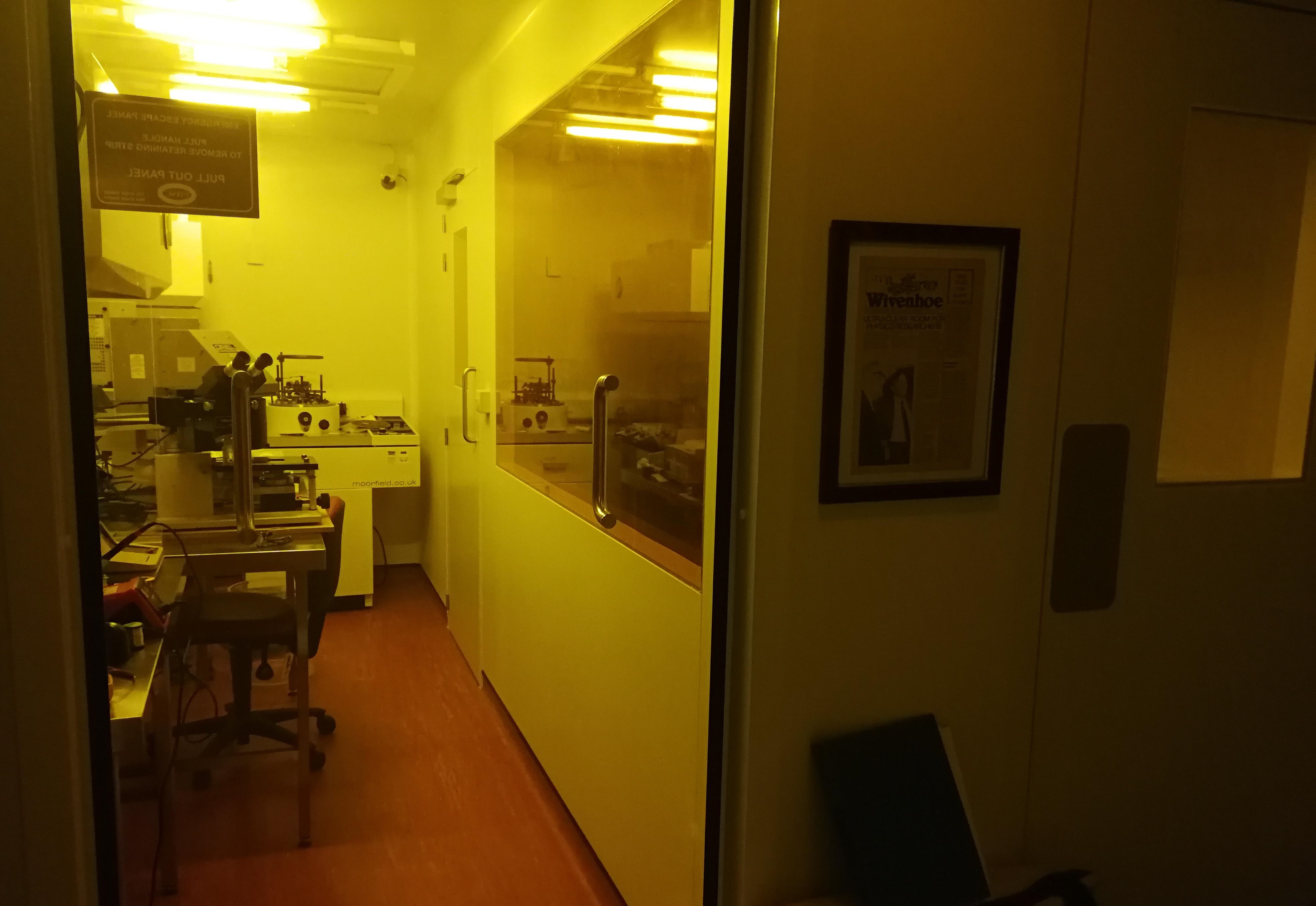
These pages provide an overview of the semiconductor device research and teaching nanofabrication facilities

Equipment

Devices Materials & Processes
Annealing Furnace   Deionised Water pin diode Lattice

Bandgap

Mask Aligner   Spincoater coplanar waveguide Etching 
Surface Profiler   Vacuum Coating Unit semiconductor laser Etching GaN


Wirebonder AFM Polysilicon Plasma
Journals Online Links

 Device Modelling with Dessis 9

 Papers & Posters

References 

 Robotics

Four-Point Probe 

Laser safety

The Science Workshop

Computer Aided Design

Software

Optical Fibre

Photomasks
Reticules

The Department of Computing & Electronic Systems

Nanofab | These pages are written & maintained by Adrian Boland-Thoms | email Adrian

Any errors on these pages are solely the responsibility of the author

Latest Additions and Revisions 3rd December 2021

eXTReMe Tracker